- JMP will suspend normal business operations for our Winter Holiday beginning on Wednesday, Dec. 24, 2025, at 5:00 p.m. ET (2:00 p.m. ET for JMP Accounts Receivable).
Regular business hours will resume at 9:00 a.m. EST on Friday, Jan. 2, 2026. - We’re retiring the File Exchange at the end of this year. The JMP Marketplace is now your destination for add-ins and extensions.
- Subscribe to RSS Feed
- Mark Topic as New
- Mark Topic as Read
- Float this Topic for Current User
- Bookmark
- Subscribe
- Mute
- Printer Friendly Page
Discussions
Solve problems, and share tips and tricks with other JMP users.- JMP User Community
- :
- Discussions
- :
- Need the Add-in JSL script to plot wafer map.
- Mark as New
- Bookmark
- Subscribe
- Mute
- Subscribe to RSS Feed
- Get Direct Link
- Report Inappropriate Content
Need the Add-in JSL script to plot wafer map.
Dear Sir or Ma'am,
Could you please get the Add-in JSL (JMP script) to construct the wafer map based on the value of each X/Y cell (either “0” Red or”1” green) for me?
I have already had the X and Y coordinate and Value of each test- either 1 (Pass) or 0 (Fail).
Thanks,
John
- Mark as New
- Bookmark
- Subscribe
- Mute
- Subscribe to RSS Feed
- Get Direct Link
- Report Inappropriate Content
Re: Need the Add-in JSL script to plot wafer map.
- Mark as New
- Bookmark
- Subscribe
- Mute
- Subscribe to RSS Feed
- Get Direct Link
- Report Inappropriate Content
Re: Need the Add-in JSL script to plot wafer map.
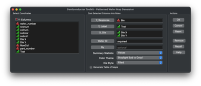
Hey! If you stack your data so that the different tests are in one column and the result in a second (Test and Bin in the attached data table). You can use the Semiconductor toolkit to generate these figures:
using these settings:
In the Patterned Wafer Map Tool
Best,
M
- Mark as New
- Bookmark
- Subscribe
- Mute
- Subscribe to RSS Feed
- Get Direct Link
- Report Inappropriate Content
Re: Need the Add-in JSL script to plot wafer map.
Hi Mike,
Great. Would you please provide me a link to download the link to Semiconductor toolkit?
Thanks,
John Wang
- Mark as New
- Bookmark
- Subscribe
- Mute
- Subscribe to RSS Feed
- Get Direct Link
- Report Inappropriate Content
Re: Need the Add-in JSL script to plot wafer map.
Someone put it in an earlier comment. And it's in the file exchange part of the community in the add-in's section. It's one of the featured add-ins.
M
Recommended Articles
- © 2025 JMP Statistical Discovery LLC. All Rights Reserved.
- Terms of Use
- Privacy Statement
- Contact Us


