- New to JMP? Let the Data Analysis Director guide you through selecting an analysis task, an analysis goal, and a data type. Available now in the JMP Marketplace!
- See how to install JMP Marketplace extensions to customize and enhance JMP.
- Subscribe to RSS Feed
- Mark Topic as New
- Mark Topic as Read
- Float this Topic for Current User
- Bookmark
- Subscribe
- Mute
- Printer Friendly Page
Discussions
Solve problems, and share tips and tricks with other JMP users.- JMP User Community
- :
- Discussions
- :
- Re: How to determine clusters of semiconductor wafer defect / sort patterns?
- Mark as New
- Bookmark
- Subscribe
- Mute
- Subscribe to RSS Feed
- Get Direct Link
- Report Inappropriate Content
How to determine clusters of semiconductor wafer defect / sort patterns?
HI,
I have just recently installed JMP 12.
One of the main reasons I did so was to improve our data mining capabilities by possibly using the "Clustering Improvements" introduced in JMP 12.
My basic need is to divide wafer patterns into groups in order to perform a commonality analysis with the intention of finding the sources of variation.
As stated in the JMP 12 release notes:
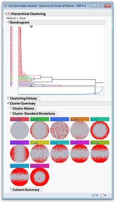
"In the semiconductor and other industries, it is important to determine clusters of wafer defect patterns. This previously meant creating one variable to make XY coordinates, then splitting on this dimension, clustering, and merging the clusters. Now, JMP accomplishes this in one step."
There is an illustration showing an example of what I would like to do:
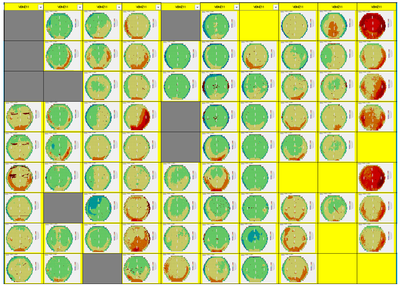
I have a need to perform such analyses quite often. An example from this week is seen below:
I need to determine how many similar patterns exist and how many wafers belong to each pattern?
Has anyone performed such an analysis?
Is there a good tutorial / guide available anywhere?
I am sure that this is of major interest to semiconductor and MEMs device manufacturers.
This case could be a good candidate for some forthcoming JMP Discovery Summit
All advice and input is appreciated.
- Philip
Accepted Solutions
- Mark as New
- Bookmark
- Subscribe
- Mute
- Subscribe to RSS Feed
- Get Direct Link
- Report Inappropriate Content
Re: How to determine clusters of semiconductor wafer defect / sort patterns?
Yeah... This is an awesome feature in 12, but its a little light in the documentation. The basics of how to use it (with the wafer maps of the clusters) is as follows (Note that you need a count column - i.e. defects in a die - and x-y coordinates for the structure of interest - i.e. die location - to make this work.):
- In JMP12 go to Analyze > Multivariate Methods > Clustering.
- Put the column of data that contains your defect count in Y
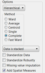
- Select the drop down in the lower left corner of the dialog that says "Data as usual." Choose "Data is stacked" from this drop down menu.
- Check "Add Spatial Measures" below the drop down list (will appear after selecting "Data is stacked").
- Add the x and y coordinates of the structure of interest to the Attribute ID area of the dialog.
- Add wafer Identifies to the Object ID area (i.e. Lot ID, Wafer ID, Slot ID, etc. or combinations of these).
- Click OK.
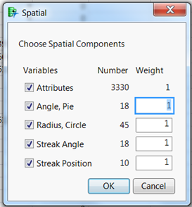
- In the next dialog you can adjust the weightings of the different spatial components in the analysis. (I'd just go with the defaults for now)
- Click OK.
- The report will now show the dandrogram where you can tune the number of clusters you want to consider. You can adjust this using the small diamond on the x-axis of the dendrogram.
- To see the clusters as wafer maps you select "Cluster Summary" from under the red arrow at the top of the report. The report will also output a data table with the clusters as pictures in an expression column.
Hope that helps!
best,
M
- Mark as New
- Bookmark
- Subscribe
- Mute
- Subscribe to RSS Feed
- Get Direct Link
- Report Inappropriate Content
Re: How to determine clusters of semiconductor wafer defect / sort patterns?
Hi, Philip!
You are correct; this issue has been, is, and will be of major interest to semiconductor device manufacturers. For instance, SEMATECH sponsored an entire Statistical Methods Symposium on spatial statistics way back in 1999. I know of no great tutorials or guides specifically about spatial statistics in semiconductors...I surmise that is due, in part, to the competitive advantage a theoretically-justified and well-working system would bestow upon the owner. Intellectual property is highly valued in that industry.
Perhaps you would be interested in this JMP Discovery 2014 presentation: https://community.jmp.com/servlet/JiveServlet/download/6695-5-69366/Semiconductor%20Wafer%20Spatial%...
It is said at the beginning of every Star Trek episode: Space really is the final frontier! Good luck!
- Mark as New
- Bookmark
- Subscribe
- Mute
- Subscribe to RSS Feed
- Get Direct Link
- Report Inappropriate Content
Re: How to determine clusters of semiconductor wafer defect / sort patterns?
Thanks Kevin,
A great and informative article.
Exactly the type of work I would like to do.
Unfortunately the techniques are not shared
Best Regards,
Philip
- Mark as New
- Bookmark
- Subscribe
- Mute
- Subscribe to RSS Feed
- Get Direct Link
- Report Inappropriate Content
Re: How to determine clusters of semiconductor wafer defect / sort patterns?
There was a presentation given in 2014 on a similar topic. You could check this out and see it it helps. It doesn't have the full answer, but you could see if it takes you down the right path. It was designed to look at sort spatial patterns:
Semiconductor Wafer Spatial Pattern Classification With JSL
-Carl
- Mark as New
- Bookmark
- Subscribe
- Mute
- Subscribe to RSS Feed
- Get Direct Link
- Report Inappropriate Content
Re: How to determine clusters of semiconductor wafer defect / sort patterns?
Thanks Carl for your input.
Best Regards,
Philip
- Mark as New
- Bookmark
- Subscribe
- Mute
- Subscribe to RSS Feed
- Get Direct Link
- Report Inappropriate Content
Re: How to determine clusters of semiconductor wafer defect / sort patterns?
Yeah... This is an awesome feature in 12, but its a little light in the documentation. The basics of how to use it (with the wafer maps of the clusters) is as follows (Note that you need a count column - i.e. defects in a die - and x-y coordinates for the structure of interest - i.e. die location - to make this work.):
- In JMP12 go to Analyze > Multivariate Methods > Clustering.
- Put the column of data that contains your defect count in Y
- Select the drop down in the lower left corner of the dialog that says "Data as usual." Choose "Data is stacked" from this drop down menu.
- Check "Add Spatial Measures" below the drop down list (will appear after selecting "Data is stacked").
- Add the x and y coordinates of the structure of interest to the Attribute ID area of the dialog.
- Add wafer Identifies to the Object ID area (i.e. Lot ID, Wafer ID, Slot ID, etc. or combinations of these).
- Click OK.
- In the next dialog you can adjust the weightings of the different spatial components in the analysis. (I'd just go with the defaults for now)
- Click OK.
- The report will now show the dandrogram where you can tune the number of clusters you want to consider. You can adjust this using the small diamond on the x-axis of the dendrogram.
- To see the clusters as wafer maps you select "Cluster Summary" from under the red arrow at the top of the report. The report will also output a data table with the clusters as pictures in an expression column.
Hope that helps!
best,
M
- Mark as New
- Bookmark
- Subscribe
- Mute
- Subscribe to RSS Feed
- Get Direct Link
- Report Inappropriate Content
Re: How to determine clusters of semiconductor wafer defect / sort patterns?
Hi Michael,
Thank you so much for your input.
I have tried to make the analysis as you instructed and have even managed on a few occasions
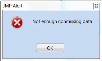
However I quite often get the Alarm message below which brings the analysis to an abrupt and .
Any idea what may cause this?
Are there any limitations on the data type?
It looks however very promising and I will continue to evaluate / investigate.
Is there any further documentation on this technique?
Best Regards,
Philip
- Mark as New
- Bookmark
- Subscribe
- Mute
- Subscribe to RSS Feed
- Get Direct Link
- Report Inappropriate Content
Re: How to determine clusters of semiconductor wafer defect / sort patterns?
Phillip,
That's a different problem entirely. Can you tell us some more about your data set? Maybe post an anonymized version of the data? What is probably happening is that you are trying to split the data in too many subgroups. This has happened to me in the instances where I have a very wide (many columns), but shallow (few rows) data set. If you are doing semiconductor defect data (like the non-JMP map you provided) then I'm betting the error you are seeing is more about trying to cluster on too many potential causal clusters. Can you provide some details?
Best,
M
- Mark as New
- Bookmark
- Subscribe
- Mute
- Subscribe to RSS Feed
- Get Direct Link
- Report Inappropriate Content
Re: How to determine clusters of semiconductor wafer defect / sort patterns?
Hi Michael,
Thank you for your response. I was using only one Defect Count column at the time.
After restarting JMP I am no longer seeing the intermittent Alarm message.
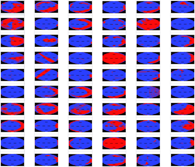
I have been able to run the analysis following your instructions. See an example below:
Due to the documentation being "a little light" on this feature I was wondering if you could help explain when to use Ward, .. Average, .. Complete Options?
Also, can you explain the significance of Number and Weight in the Spatial Components?
When viewing the types of wafermaps I have coming off the line (see above), do you have any recommendations for these Component settings?
- Philip
- Mark as New
- Bookmark
- Subscribe
- Mute
- Subscribe to RSS Feed
- Get Direct Link
- Report Inappropriate Content
Re: How to determine clusters of semiconductor wafer defect / sort patterns?
Philip,
Hi! Glad you got that figured out! On these two new questions, the details on the different fitting methods are described in detail in the books that come with your install of JMP. The one you want is the Multivariate Methods book. Its found under Help > Books > Multivariate Methods. The details about the fitting methods are found in the Statistical Details for Hierarchical Clustering section, found starting on page 75.
On your second question regarding the Spatial Components. The numbers are the number of potential spatial components that the analysis found (it already does some preliminary work at this point).
- Attributes are the specific combinations of the variables provided in the attributes field of the set up dialog. In this case that would the the individual die as defined by the (X,Y) coordinate pairs.
- Angle, Pie looks for wedge shapes or hemispherical shapes (i.e. one half of a wafer gets decorated with Cu nodules due to a faulty connection with the plating electrodes or something).
- Radius, Circle looks for things like ring scratches in CMP, or maybe CVD based patterns with a shower head deposition set up.
- Streak, Angle looks linear features that have the same angle (i.e. streaks from a faulty Marangoni drying set up.)
- Streak, Position looks for streaks with a similar position spatially.
You can see what each of the features looks like in the data table provided when this "Spatial" dialog pops up. It will show the Hough transform for each of the variables in the dialog along with other information about each feature. You can decide which to include by checking on unchecking the the check boxes next to each feature type in the dialog, i.e. if you aren't concerned about ring scratches in this analysis, uncheck the variable type that has those features based on the Hough transform information - probably Radius, Circle.
The weighting in the Spatial Dialog is exactly what it sounds like: it weights the importance of each variable type in the clustering analysis. If something needs to be considered, but is less important than a particular feature type, you can make it less important than other feature types.
On your last question about settings, I'd base settings on what you see in the Hough transforms, the dialog (counts of each feature type), and what you know about the line. If you know you've got material still in the line impacted by a streaking problem dialing down the weight of the steaks might be prudent. You probably want to monitor for recurrence but don't want to be chasing your tail about something you already know about. If you don't care about streaks at all, turn them off entirely. My basic recommendation on this type thing is to use the defaults until you've got data - numerical or circumstantial - to do otherwise.
Best,
M
Recommended Articles
- © 2026 JMP Statistical Discovery LLC. All Rights Reserved.
- Terms of Use
- Privacy Statement
- Contact Us

