cancel
Showing results for 
Show  only  | Search instead for 
Did you mean: 
JMP is taking Discovery online, April 16 and 18. Register today and join us for interactive sessions featuring popular presentation topics, networking, and discussions with the experts.
Choose Language Hide Translation Bar
Striving for zero-defect products

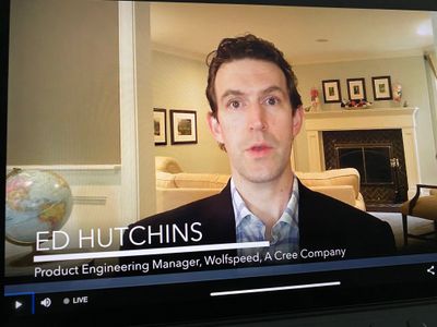
Ed Hutchins, Wolfspeed, outlines the new and powerful ways engineers are striving to create zero-defect products.Ed Hutchins, Wolfspeed, outlines the new and powerful ways engineers are striving to create zero-defect products.Organizations are embracing more automation and the rise of the digital economy in the production and delivery of products. And with in-line sensors afforded by the rise of the Industrial Internet of Things (IIoT) and advanced measurement systems, they are generating and collecting a growing volume of data that is more complex than ever before. Ed Hutchins, Product Engineering Manager at Wolfspeed, A Cree Company, explains in this video clip. You can watch the complete panel conversation on demand.

“I started talking about that earlier, about the massive amounts of data, but that’s just the start of it. I think the way that data is being used is changing, and it’s changed very recently. It used to be with automated inspection tools, you’d define recipes to look for specific features, specific attributes, specific defects.

"But now with the advent of machine learning and deep neural networks, you’re able to create an algorithm that looks for a defect that you can see by eye but would have a hard time reducing to a finite set of parameters or a recipe for instruction.

"And what these things are allowing us to do is to find defects that otherwise would have required human intervention or sampling, and now we can look at the whole picture.

"We can look at the whole product, we can look at every wafer, we can look at every example to try to find these features as a way for striving for zero defect, which, again, is part of the expectation of our customers these days.”

Here's a preview of the on-demand webcast:

Last Modified: Jul 22, 2020 8:19 AM
Comments
sajid
Level I

So few questions after learning about the massive data generated by machine learning & neural networks helping in identifying defects of interest in semi-process manufacturing.

1) with the conventional approach of using (AOI) Automated-Optical systems detecting inline defects among various process steps, we only focus on the killing defects which might fails dies at the wafer-level or product level and so that reason we strategically place inspection recipes in the most critical areas of interest. In order to use our manufacturing process resources in most efficient manner, what we avoid is to capture non-killing defects. As per machine learning algorithms and looking a specific defect, which could be in critical or non-critical areas on all wafers, does that jeopardize cycle time? Does it show high correlation coefficient with functional and product failures?

2) keeping the focus on the defect reduction and customer expectations, does the (D0) methodology is focus on eliminating all defects? if so, is it cost effective than the current practice of using AOI?

3) could you share some nonproprietary data to show some correlations based on this methodology?


Thanks!


/Sajid Shamsi

J_Marquardt
Staff

Hi @sajid -


We reached out to Ed Hutchins so that he could respond directly. Here's what he said:


1) In our experience, the use of machine learning algorithms to identify killing defects can be implemented such that it does not add appreciable cycle time to the process compared to AOI systems.  To achieve this, though, one has to set up a system with several practical elements in mind: how much data is generated by the inspection system, how powerful is the computer that will be running the machine learning algorithm, and where is that computer relative to the inspection system.   If those elements are considered and the system is designed appropriately, the whole process can run quickly, from seconds to a few minutes per wafer depending on how much data must be analyzed.  When trained properly, a machine learning algorithm is very accurate, and we see direct correlation between its findings and downstream product attributes or failures.


2) Zero-defect and automated defect detection are complimentary.   100% inspection is much less costly and time consuming when enabled with automated inspection equipment and machine learning algorithms.  These systems do two things to promote zero-defect: they promote downstream yields by preventing any defects from passing into products, and they enable upstream improvement activities by accurately describing the occurrence of defects, even those that appear infrequently.


3) Dr. Robert Leonard from Wolfspeed presented an application of machine learning at the 2019 Internal Conference on Silicon Carbide and Related Materials (ICSCRM).  When the conference proceedings are published, his paper will contain example images demonstrating correlations.