- New to JMP? Let the Data Analysis Director guide you through selecting an analysis task, an analysis goal, and a data type. Available now in the JMP Marketplace!
- See how to install JMP Marketplace extensions to customize and enhance JMP.
- Subscribe to RSS Feed
- Mark Topic as New
- Mark Topic as Read
- Float this Topic for Current User
- Bookmark
- Subscribe
- Mute
- Printer Friendly Page
Discussions
Solve problems, and share tips and tricks with other JMP users.- JMP User Community
- :
- Discussions
- :
- Re: wafer map
- Mark as New
- Bookmark
- Subscribe
- Mute
- Subscribe to RSS Feed
- Get Direct Link
- Report Inappropriate Content
wafer map
I want to konw how to make wafer map with JMP.
Accepted Solutions
- Mark as New
- Bookmark
- Subscribe
- Mute
- Subscribe to RSS Feed
- Get Direct Link
- Report Inappropriate Content
Re: wafer map
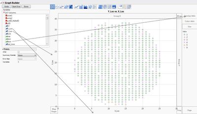
I normally use Graph Builder to do this.
It really depends on what type of data you looking for. For example, i often use this to check my Wafer testing (Chip Probe , SORT) hard bin results.
1. Put X-Loc to X-axis
2. Put Y-Loc to Y-axis
3. Put the Hardbin to Overlay
And you can see the whole wafer by its hardbin.
- Mark as New
- Bookmark
- Subscribe
- Mute
- Subscribe to RSS Feed
- Get Direct Link
- Report Inappropriate Content
Re: wafer map
Use the X-Y plot
- Mark as New
- Bookmark
- Subscribe
- Mute
- Subscribe to RSS Feed
- Get Direct Link
- Report Inappropriate Content
Re: wafer map
I have put some old code at:
https://community.jmp.com/docs/DOC-7137
that may be worth a look. There are many alternatives, particularly if you are prepared to use JSL.
- Mark as New
- Bookmark
- Subscribe
- Mute
- Subscribe to RSS Feed
- Get Direct Link
- Report Inappropriate Content
Re: wafer map
I think the answer depends on what type of wafer map you're looking for. The script that Ian@JMP linked seems to be a good option for parametric wafer maps.
If you're looking to build a bin classification wafer map, then the built-in platform that I've found to be most useful is Bubble Plot. A few tips when using Bubble Plot to make wafer maps:
- Change shape to square for a more "die-like" appearance
- Use Column Properties to set standard properties:
- X/Y orientation with Value Ordering
- Bin Colors with Value Colors
- Label is whatever classification you want to show, such as a bin number
I've also managed to create some interesting - what I've termed - Hyper-heat maps. By creating custom maps to represent sub-die structures, you can then use Graph Builder to make X-Y arranged wafer maps of these heat maps, i.e. a hyper-heat map. For complex SOCs, this can be a powerful visualization technique.
And, as always, nearly anything is possible using custom-built JSL scripts.
- Mark as New
- Bookmark
- Subscribe
- Mute
- Subscribe to RSS Feed
- Get Direct Link
- Report Inappropriate Content
Re: wafer map
For Bin maps : X/Y plot with Graph Builder. Using wafer id and the wrap function, all wafers from a lot can be displayed together.
For parametric maps : Graph Builder (same as above); Contour Plot.
- Mark as New
- Bookmark
- Subscribe
- Mute
- Subscribe to RSS Feed
- Get Direct Link
- Report Inappropriate Content
Re: wafer map
Hi Murphy,
Do you have an example code of what you mention ?
Thanks
- Mark as New
- Bookmark
- Subscribe
- Mute
- Subscribe to RSS Feed
- Get Direct Link
- Report Inappropriate Content
Re: wafer map
I normally use Graph Builder to do this.
It really depends on what type of data you looking for. For example, i often use this to check my Wafer testing (Chip Probe , SORT) hard bin results.
1. Put X-Loc to X-axis
2. Put Y-Loc to Y-axis
3. Put the Hardbin to Overlay
And you can see the whole wafer by its hardbin.
- Mark as New
- Bookmark
- Subscribe
- Mute
- Subscribe to RSS Feed
- Get Direct Link
- Report Inappropriate Content
Re: wafer map
You can simply use graph builder to make wafer maps.
use N View Levels( 4 ),First View Level( 1 ) to arrange in columns and rows
then append all views one by one.
N View Levels( 4 ),First View Level( 2 )
- Mark as New
- Bookmark
- Subscribe
- Mute
- Subscribe to RSS Feed
- Get Direct Link
- Report Inappropriate Content
Re: wafer map
Use the Semiconductor Toolkit: https://community.jmp.com/t5/JMP-Add-Ins/Semiconductor-Toolkit/ta-p/22460
M
Recommended Articles
- © 2026 JMP Statistical Discovery LLC. All Rights Reserved.
- Terms of Use
- Privacy Statement
- Contact Us


