- Browse apps to extend the software in the new JMP Marketplace
- This add-in is now available on the Marketplace. Please find updated versions on its app page
- Subscribe to RSS Feed
- Mark as New
- Mark as Read
- Bookmark
- Subscribe
- Printer Friendly Page
- Report Inappropriate Content
JMP Add-Ins
Download and share JMP add-ins- JMP User Community
- :
- File Exchange
- :
- JMP Add-Ins
- :
- Semiconductor Toolkit
Hi, @MikeD_Anderson , @JinyoungLee , @Yngeinstn
Thank you for your help.
I've solved the problems and could make the wafer map I want.
Now I know the STK is just Mike's personal project, but I have another question about STK.
Could you please help me one more time ?
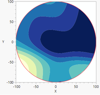
- How can I make the Legend or interconnect the color of legend (and range) with JMP Graph, such as Figure 2.
- Can I delete the value in the die of wafer map?
- Can I zoom or fit the size of wafer map?
- How many dies can be handled in the current version?
Thanks again,
HK Jung
Do you have any recommendations when it comes to something like this? I know you said this didn't didn't have the capability for pizza/jigsaw wafer and gave me some suggestions but i am really struggling here.. This is seriously the bane of my existence. At this point i think i am truly out of luck..
Thanks in advance
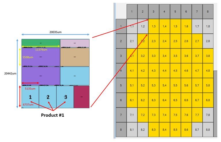
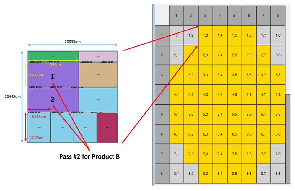
The problem here is the layout. The only way that I could think of to map this is to first generate a shapefile or coordinates for the field layout than transpose that across the shot map. It’s not something the STK is currently set up to do. If you had the coordinates of the corners for each of the sub-chips you could write some JSL to create the translations. That’s about the best solution that I can think of at the moment.
Sorry I can’t be more help on this one,
M
No worries.... If i can't figure this out then the designers will have to live with what i can actually do..
Thanks
I am trying to use semiconductor toolkit, I opened a table, and when I click the toolkit, nothing happened.
could you please advise?
Hi, @Ally,
Can you open the log window and see if there are any messages there? Also what version of JMP are you running?
Thanks,
M
Hi, @MikeD_Anderson
I'm sorry to confuse you.
I have 4 questions.
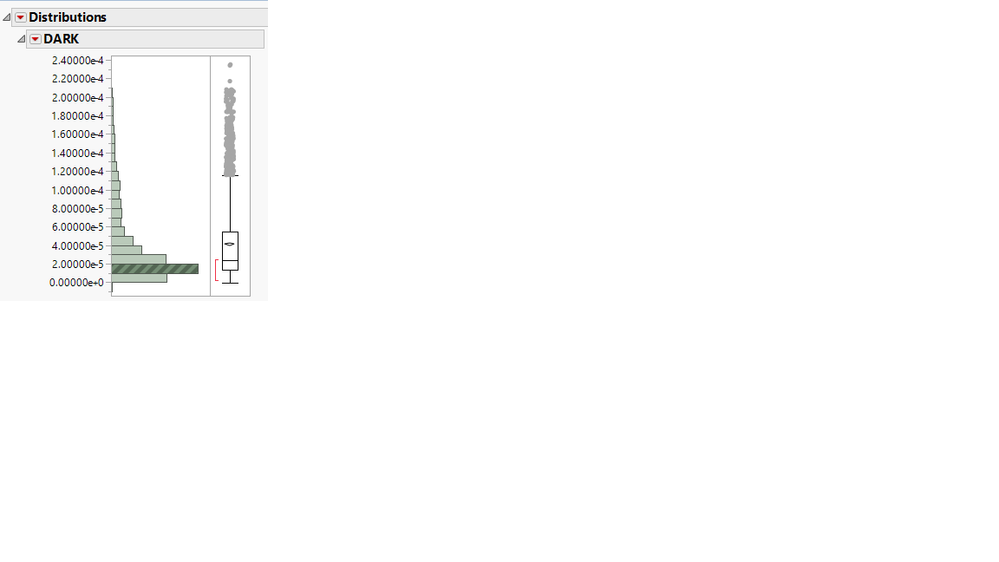
1. I want to know how to make a legend, which is connected to the JMP distribution graph, on the wafermap. (JMP graph, figure2, means the distribution graph.)
2. Can I delete the value in the die of wafer map, such as count, range, mean and so on.
3. Can I zoom or fit the size of wafermap?
4. How many dies can be handled in the current version of semiconductor toolkit?
The JMP Korea's Senior Systems Engineer says the three functions (Q1, Q2, Q3) may be possible, and there is no limit of the number of die, but I'm little confused about whether he talks about JMP or STK. So I'll try to explain to JMP Korea's engineer in detail what I want from this tool.
I really appreciate JMP's support.
Thanks,
HK
Hi! Thanks for the clarification. On your questions see below.
- I want to know how to make a legend, which is connected to the JMP distribution graph, on the wafer map.
- This is possible, but the STK isn't set up to do this at the moment. I'll put it on the request list for the next release.
- Can I delete the value in the die of a wafer map, such as count, range, mean and so on?
- This is possible, but a little technical. If you right-click on the graph you will see an option that says "customize". In the customize menu, there is an entry for Die and Labels. This graphic script contains an entry "Text(...)." If you delete that entry the labels will disappear. I'll also add a request to my list to make this easier.
- Can I zoom or fit the size of the wafer map?
- You can adjust the size of the map by dragging on the edges of the x- and y-axes on the graph.
- How many dies can be handled in the current version of semiconductor toolkit?
- My counterpart is correct, there is no limit to the number of die or wafers that the STK can handle. Practically, there will be a point where legibility will become an issue, which is a bigger concern in my book.
Hope that helps!
Best,
M
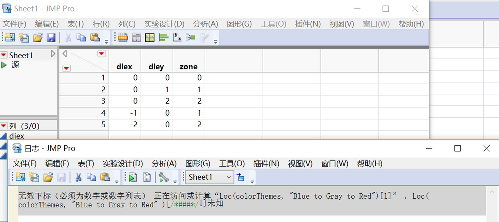
I am using JMP 14.2 version and below is the log, while it is in Chinese. It is saying: invalid subscript (has to be number), it is accessing or calculating ''Loc(..."
Thanks! That's informative. I have a suspicion it has to do with the fact that you're running JMP in Chinese. Can you do the following for me?
- Open a script window (File > New > New Script).
- Paste this command: Get Color Theme Names();
- Select Edit > Run Script.
- Look in the log and send me the list that shows up.
best,
M
Thanks for the instruction, Mike. Here is the output, while unfortunately, it is all Chinese charactors, all kinds of colors.
Does this help?
//:*/
Get Color Theme Names();
/*:
{"由绿经黑到红", "由绿经白到红", "由白到黑", "由蓝经灰到红", "由蓝经绿到红", "光谱", "由蓝经青黄橙到红", "由白到蓝", "由白到绿",
"由白到红", "JMP 默认", "JMP 深色", "JMP 浅色", "浓重", "成对", "柔和色", "普通", "SAS 默认", "SAS 浅色",
"SAS 统计", "SAS 分析", "JMP 鲜艳", "冷色变暖色", "蓝白红", "绿色变紫色", "青色变棕色", "白色变橙色", "白色变紫色",
"黄色变红色", "黄色变蓝色", "Viridis", "Magma", "黑体", "紫绿色", "柔黄色变红色", "绿黄红", "暗灰色", "浓淡混合"}
That’s what I was afraid of. The STK is looking for a color theme in English. With the color theme names being in Chinese, it’s not able to find what it’s looking for and crashing out. I’m not sure how to work around this beyond turning on the English language localization.
M
Hi @MikeD_Anderson,
I just installed the toolkit, however I am unable to launch it. When I launch it, nothing happens & I get the following error (from log):
Unknown
The following objects failed to initialize and have been removed from the application. This might be due to data table dependencies that are not fully satisfied, or other causes. Additional details might be available in the log.
Objects
annotateTab
annotateBox
winListObx
basisObx
colorsObx
mapTab
mapBox
analysisTab
analyzeBox
UtilityTab
utilityBox
creditTab
credBox
Please help. I am running JMP Pro 12.2.0. Is there a file I need to pre-load before I run the App?Appreciate your help!
Thanks
There’s been another JMP 12 user that had that same error. I wasn’t able to run it down. The current version of the software was released on JMP 14 and I never tested it on JMP 12. I’d start by asking your license administrator about getting JMP Pro 14. Depending on your license, it’s probably a free upgrade.
M
Hi Anderson @MikeD_Anderson ,
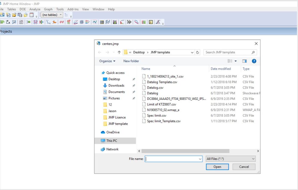
I just installed toolkit in JMP12, looks like it doesn't work.
When I click the toolkit, one window named "centers.jmp" occurs, and no other window occurs;
Can you please explain the procedures and steps? Like how to install and what next?
Thanks a lot !
Sarath.
M
hello:
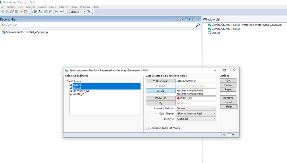
I want to use the add-in to draw "Patterned Wafer Map", but when I press the X.Die buttion,it don't work, can you help me ? thank you!
If you’re in the annotate tool (look at the buttons along the top), you need to create a visualization using graph builder or contour map first. Have a look at the pdf there are examples of what each tool does.
Best,
M
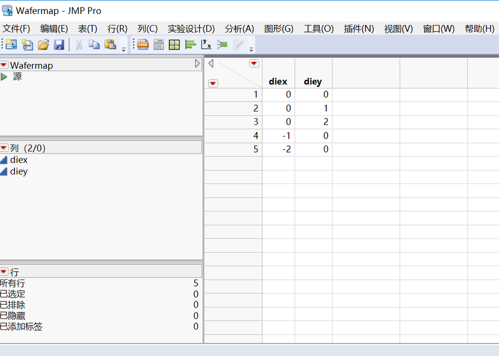
Edit - @sxwxw5191 - I just looked at the picture you sent. The tool that you are trying to use requires that the data be the numeric ordinal modeling type (green icon). If you right-click on the blue triangles next to the columns and select "ordinal" it should work. - M
Hi Mike,
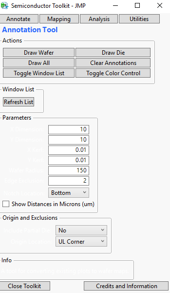
I am using JMP 14 (64 bit), and I have installed add-in of semicondcutor toolkit.
I realize the interface shows blank except buttons as a figure shows below.
Do you any suggestion to fix it?
@KSW - Hi! It looks like a correction that I made so that the application would work with dark mode on Mac OS isn't playing nice with JMP 14 on windows... I uploaded the old version (it has JMP14 in the file name). Try that one and it should behave.
Best,
M
Hi everyone,
Any issues running STK on JMP15.1? When trying to create a wafer map got the error message below.
Thanks for the help.
EC
@Enio_Carpi - nope the STK is fine in 15.1. That's just a bug I haven't got around to fixing yet. Sorry!
M
Hi Mike,
This add-in looks pretty useful Mike. I think I personally know txnelson and miss working with him. He had created some nice tools along these lines.
In terms of suggestions for an update, I have the following to contribute. Defect data usually comes in a file type called a Klarf file. I have most of the code needed to parse and plot the Klarf file, label the notch location, and draw the wafer around the map. It allows the user to choose individual plots for each wafer, or to have one graph with smaller images of each wafer tiled for all the wafers in a lot. Marker size is scaled by defect size, and color scaled by image contract. I need to do some bug fixes. After the most recent JMP summit, I was made aware that images can be embedded in JMP tables. The images from the defect review usually come in by a TIFF file that has all images in one file. It would be great if we could find a way to get meta-data, extract the defect ID, and load the image to the correct row for the defect of interest. Then data filter could be used to screen for large defects, defects with a certain contrast, etc., and defect classification type, if the tool provides that information for that defect inspection recipe.
It's still got some bugs that need to be worked on, because the Klarf file can be a pain to work with. There are a lot of nuisance rows in the input log file that have to be identified and removed, and the row count (defect count) needs to be kept track of ignoring those lines. Those lines could be useful for linking to the images.
Anyway, I think this would be a very cool addition to the add-in capabilities. I'll have to check to see if I can distribute code publicly.
@MikeD_Anderson - sorry if i missed it, but is this updated for 16? If not, do you know if/when it would be?
Working on it! ;)
We are very new to JMP! and this add-in is very interesting to us - It's mentioned above that the error I am facing is a bug - is there a workaround? Or is the functionality broken for the time being?
Thank you for your efforts!
@Enio_Carpi and @NeillSM - I just uploaded a new version that fixes that bug. Sincerest apologies for the delay!
M
Hi,
I found this semiconductor toolkit couple of days ago and it has been a great help.
I've been using it to create wafer thickness maps with Bare Wafer Map Generator, but I have couple of issues with it.
- Our wafers have flats instead of notch. It would be great if there was an option to draw flat.
- Bare Wafer Map Generator draws the notch to bottom as default. It would be great to have to those notch location parameters available also in the generator. Now I can draw the notch after the generation with annotation tool, but it would be handier to have that option in generator. Also the color control in the generator would be good.
Thanks!
@MarkoJ - Hi! Thanks for the thoughts. I was taking a break from working on the next version of the STK when I saw your note... so, great timing! I wonder if you could pm me with some examples of what you'd be looking for in the flat marker and orientation control. I'd also like to hear about what you're looking for in terms of the color control.
Thanks!
Mike Anderson
This is a very useful toolkit but it is in need of an update as already noted. Hopefully, that's not too far away.
I really appreciate this tool and would be excited to see the following features added. Some have already been mentioned. I'm mentioning them again to hopefully improve their priority in the feature list.
- ability to save a different default "wafer radius" and "exclusion zone" in the Wafer Parameters section
- ability to show notch/flat and orient it up/down, left/right or by degree
- ability to show show location of actual data points and not just the "data points" used in the "fitting and display parameters" fit
- fix the graph to be a perfect square regardless of window size. This way the wafer edge display always aligns with the wafer map. Currently the wafer edge is always a perfect circle but the map follows dimensions of the window causing the two to not be aligned until the user very specifically sizes the window for perfect alignment
Thank you.
Al
- Ability to save a different default "wafer radius" and "exclusion zone" in the Wafer Parameters section
- In progress for the v16 release.
- Ability to show notch/flat and orient it up/down, left/right or by degree
- In progress for the v16 release.
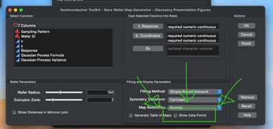
- Ability to show show location of actual data points and not just the "data points" used in the "fitting and display parameters" fit
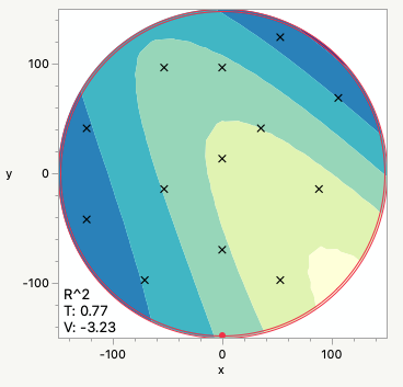
- This can already be done using the checkbox in the lower left of the launch dialog. You're trying to use the one that's native to contour plot - I have no control over that.
- This can already be done using the checkbox in the lower left of the launch dialog. You're trying to use the one that's native to contour plot - I have no control over that.
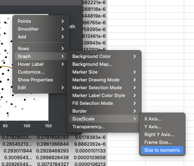
- Fix the graph to be a perfect square regardless of window size. This way the wafer edge display always aligns with the wafer map. Currently the wafer edge is always a perfect circle but the map follows dimensions of the window causing the two to not be aligned until the user very specifically sizes the window for perfect alignment
- Sometimes JMP decides to resize thing on its own. I have no control over this. The easiest thing to do is just use the Size to Isometric function that's in every window. This is what I already do as part of the scripts, but sometimes it get's overridden or changed later by JMP…
- Sometimes JMP decides to resize thing on its own. I have no control over this. The easiest thing to do is just use the Size to Isometric function that's in every window. This is what I already do as part of the scripts, but sometimes it get's overridden or changed later by JMP…
@MikeD_Anderson Thank you for showing the "Size to Isometric" feature but when I check the "Show Data Points" in the "Fitting and Display Parameters" like you showed, I don't see them. I reverted to overlaying an X,Y scatter plot of the data points on to my map in Powerpoint. What is this supposed to look like? Here's a sample map I get with the "Show Data Points" enabled. It looks just like when "Show Data Points" is not enabled for me. I tried different color themes for the gradient just to make sure I wasn't missing anything and still don't see any data points.
I'm using JMP 16.0.0
Thank you.
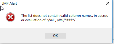
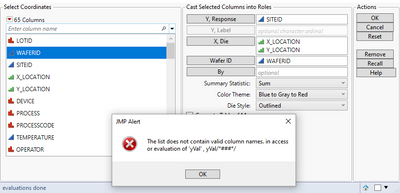
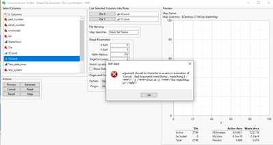
Would anyone have an idea on how to get around this JMP alert?
I am using the Die Index option and filling the x and y coordinates with an ordinal column. The preview button seems to work, but clicking generate pops this window up
Hello Mike,
Thanks for sharing this addin. I tried to install this addin, but there is no sub-script appeared as attached pic.
Thanks!
Yun
Hi Mike
Is STK running on 16.1?
Mike: this tool is exactly what Im looking for.
Im on JMP 13 as my laptop has windows 7 and I cant upgrade to a higher version of JMP. Where do I find the semiconductor plugin compatable with JMP13?
Thanks
Hi, @JIcuss - I started developing the toolkit for JMP 14, so there isn't a version that supports 13.
Sorry,
M
- Mark as Read
- Mark as New
- Bookmark
- Get Direct Link
- Report Inappropriate Content
Hello,
I was just wondering if it is possible to import a die map from a design file (specifically a gds file) to JMP.
my plan is to import files made on Klayout to JMP
Please let me know if this is possible and how can I go about doing this
Best Regards
Haroon Shahbaz
Is there a way to use a GDS file to create a die map? I'm looking to stack defect coordinates to in-die locations.
Thanks
@DecileOcelot503 and @EnioC ,
Thanks for the interest in the STK. It doesn't support GDS files at the moment. Mostly because I don't have a good reference to work with to see if it's reasonable. If either of you have or can point me towards an example, I can investigate and see if it's something I can support in a future release.
Regards,
M
Hello Mike,
I would like to know if I can write a JSL script to automate the generation of wafer plots created by STK ?
At the moment, I'm using graph builder to create and save dozens of curves related to wafer characterization, and I'll love to add some drawings !
Thanks for your responds,
KInd regards,
Wafer_Lover.
@Wafer_Lover, Hi!
If you use the STK to generate shape files for graph builder, you can use those to automate.
Best,
M
Recommended Articles
- © 2026 JMP Statistical Discovery LLC. All Rights Reserved.
- Terms of Use
- Privacy Statement
- Contact Us

