- Browse apps to extend the software in the new JMP Marketplace
- This add-in is now available on the Marketplace. Please find updated versions on its app page
- Subscribe to RSS Feed
- Mark as New
- Mark as Read
- Bookmark
- Subscribe
- Printer Friendly Page
- Report Inappropriate Content
JMP Add-Ins
Download and share JMP add-ins- JMP User Community
- :
- File Exchange
- :
- JMP Add-Ins
- :
- Semiconductor Toolkit
Thanks Michael for sharing this very promising add-in!
At this point I have only tried the wafer map generator. It works well for the default die dimensions, but it fails when the X and/or Y dimensions are odd or fractions. For example, try with X Dimension = 25.81, Y Dimension = 15.21.
Also, the X and Y axis have wrong increment settings.
The fixes are simple:
To fix the issue with the odd / fraction die dimensions:
In MakeMainWindow, Change the definition xMax and yMax:
| //xMaX = (2 * wRad) / xSize; | ||
| //yMax = (2 * wRad) / ySize; | ||
| xMax = 2 * Ceiling(wRad / xSize); | ||
| yMax = 2 * Ceiling(wRad / ySize); |
To fix the problem with the axis increments.:
Use ySize for axisbox(1) and xSize for axisbox(2):
toolWin[Axisbox( 1 )] << Show Major Grid( 1 ) << Inc(ySize);
toolWin[Axisbox( 2 )] << Show Major Grid( 1 )<< Inc(xSize);
Lars-Åke Ragnarsson
imec
Suggestions for improvement in this tool:
- Add notch to wafer
- Add notch location (e.g. bottom, right, ...)
Lars,
Thanks for the feedback! I can't seem to generate a failure with odd sized dimensions like you describe. I'd like to get some more information about what you're experiencing. Can you send me an email at mike.anderson[at]jmp.com, please?
Thanks!
M
Thanks for these improvement suggestions. I agree with you and I'll get them into the next revision.
best,
M
fyi, Looks like the images have dissapeared ofter the migration
Yes, I was in a hurry to get the new version up, so I didn't bother with the images. I'll get them back up soon.
Best,
Does anyone know of a consultant / firm who offers custom development work of JMP solutions for fabless semiconductor companies? We are interested in using it, but would like someone with more experience to help us develop / deploy the solution. Thanks!
@mhamblin, check JMP.com/partners for a list of firms that can help you. Lots of good choices.
Does this toolkit work on jmp 12.2??
Best,
M
I tried to add this "add in" on JMP 10 version but it did not work. Is there a way to access this add in on JMP 10 version. I know, you have already mentioned, "JMP 12 or newer versions."
Thanks.
Best,
M
M
Try it now - the file open dialog should be corrected.
M
Hi M,
I am still prompted to open a file if no table is open. If a data table is selected or already open, nothing else is happening. Any way I can help troubleshoot this? (Is the download link at the top of this thread the best place to get the newest version?)
@Magic_Smoke, please make sure you have downloaded "Semiconductor Toolkit_V2-1.jmpaddin." The add-in will still ask for you to have an open data table (that's just how it works now). PM me if you're still running into issues. The add-in is provided "as is" but I'll do my best to see what the problem is.
M
Good Morning M_Andreson,
I can't download the add-ins, I got Network error. I think we have problem with the link.
Will you please fix the link?
Thank you for this wonderful add-ins
M
Yes it works. Thank you.
Hi Anderson,
I try it with JMP14, looks like it doesn't work.
Will it be updated for JMP14?
Thanks
Hello,
I would like to generate multiple wafer map shape files for different products. I generate them with "Use Geometry". The shape files for different wafer maps seem to conflict because they have the same ShapeIDs and share the same column name of "DieIndex". For my second set of shape files, I changed the ShapeID by adding 5000 for both the "Name" and "XY" files and I renamed "DieIndex" to "DieIndex2". With both sets of shape files in the SAS/JMP/13/Maps folder, they both can be used by referencing either "DieIndex" or "DieIndex2", but it seems like the presence of the second set of shape files is still influencing the first set (the x-axis scaling on my plots is different whether or not I have the second set in the Maps folders). Is there anything else I have to do such that multiple wafer maps can work independently?
Thanks,
Chris
Hi, @ChrisBrooks!
Welcome to the community! This is a fiddly problem to be sure. There may be some other solutions out there, but the one that I would recommend is to use the Map Role Column property (JMP Documentation). This lets you point your data table directly at the right product map.
There are a couple of upsides to using this method: You don't have to go directory diving for the JMP maps folder (i.e you can put it somewhere more convenient). You can also copy/paste the column property to a new dataset so you only need to set it up once.
Best,
M
Thanks for the help, it works! No need to rename any of the ShapeID's or columns if you have multiple shape files. For those who use JSL, I created a column for the "DieIndex" in my main data table whose map role property uses the shape file generated by the toolkit:
New Column( "DieIndex",
	Character( 10 ),
	Formula(Char( :DieX ) || "," || Char( :DieY )),
	Set Property("Map Role", Map Role( Shape Name Use( "C:\Users\cbrooks\Documents\Data Analysis\JMP\Semiconductor Toolkit\Die-WaferMap-Name.jmp", "DieIndex")))
);
and where I've already had made the :DieX and :DieY columns based on my particular wafer. I tried creating a variable: wafermap_shapefile = "C:\Users\cbrooks\Documents\Data Analysis\JMP\Semiconductor Toolkit\Die-WaferMap-Name.jmp"; to pass it as an argument in Shape Name Use, but it didn't work (column property had wafermap_shapefile as the file name, instead of the text string). M, what syntax am I missing to evaluate the variable as a string in Shape Name Use? By the way, my colleagues are impressed by the wafer maps but I credit you for doing all the hard work. Thanks again!
Chris
The problem with column properties is that you have to build them completely (including the file path) before trying to work on the table itself. This makes using variables tricky.
I generally try to use a combination of a column property message (i.e. col1 << set property(<stuff>)) and either a "substitute into with an expression" workflow or use the Eval(Parse()) workflow. You could also try substituting into the new column argument directly before evaluating it.
// Define the file path
wafer_shapefile = "C:\Users\cbrooks\Documents\Data Analysis\JMP\Semiconductor Toolkit\Die-WaferMap-Name.jmp";

// define the new column expression.
newCol = Expr(New Column( "DieIndex",
	Character( 10 ),
	Formula(Char( :DieX ) || "," || Char( :DieY )),
	Set Property("Map Role", Map Role( Shape Name Use( loc, "DieIndex")))
););

// back substitute the file path into the expression
Substitute Into(newCol, Expr(loc), Eval(wafer_shapefile));

// run the expression.
newCol;
Another thought (sorry for the stream of consciousness style here - caffeine hasn't kicked in yet), you could try :
// Define the file path
wafer_shapefile = "C:\Users\cbrooks\Documents\Data Analysis\JMP\Semiconductor Toolkit\Die-WaferMap-Name.jmp";

// run the column code with an evaluate arguement
New Column( "DieIndex",
	Character( 10 ),
	Formula(Char( :DieX ) || "," || Char( :DieY )),
	Set Property("Map Role", Map Role( Shape Name Use( Eval(wafer_shapefile), "DieIndex")))
);
I guess the take-home message here is that columns need some special structures to make them play nice with dynamic coding and you just have to try them to see which one works the best for a given setting.
Hope that was helpful!
Best,
M
Perfect! The first option works, second option has "Eval" as the map name data table in the map role column property.
Thanks,
Chris
Hi Anderson,
I just installed JMP14 and tried your toolkit, looks like it doesn't work.
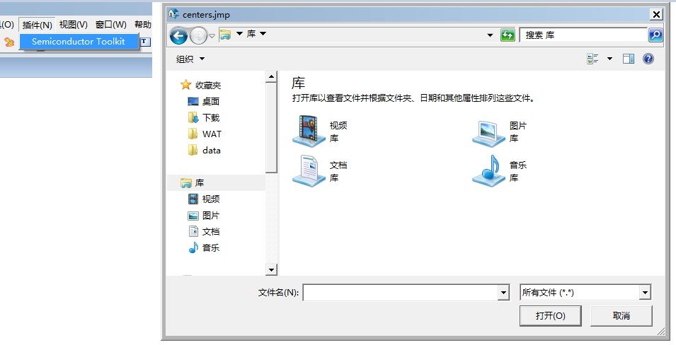
When I click the toolkit, one window named "centers.jmp" occurs, and no other window occurs;
Is it due to new version ?
Thanks a lot !
The picture
@iamshan, Hi! welcome to the community. You need to have a data table open to run the toolkit. Just open up a data table and it should behave fine.
M
Hi Anderson,
Thanks a lot! It works now ; )
WS
Hi,
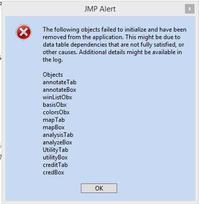
I am interested in using this Add-in, but it is not working on my system. I have JMP Pro 12.2.0 (64-bit) running, and has one other Add-in that was developed internally. I see this Semiconductor add-in under "Add-ins" but i click it and it doesn't do anything. If I click on the add-in file in the recent files list, it asks me for the center.jmp (mentioned above). I choose the jmp table i want to use and i get an error:
However, before you bother yourself with helping me fix this, i would like to know if it can manage multiple wafer maps side by side. I have parameters that I want to display with many wafers side by side (in a grid). Ideally, it'd be able to zoom in and out to get as many as 100 wafers simulataneously displayed for a quick glance, and zoom in to a few to get a more detailed breakdown.
Thanks,
Jason
@blueDevil2004, Hi! If your wafers are from the same product or die layout then you can do using a map shapefile and Graph Builder. When you start the add-in (with a data table open) you should see the main interface found on page 9 of the documentation.
I'm not 100% sure on if it will function on JMP12. I developed the latest version on JMP14 and I haven't tested it that far back.
M
Hi Mike
Thank you very much for the toolkit.
However, it doesn’t produce the wafer map I’m expecting. I have list the die numbers on the wafer, and provide the numerical coordinates in the data file, and these “numerical coordinates” is the numbering of the die on chip, for example, the 31st die was tested is located on the wafer at row 5 and column 7 is marked with DIE number of 31 and the coordinates is X=7 and Y=5, this is not the physical coordinates. However, it seems the semiconductor toolkit asks the coordinates of the dies are based on the physical measures. I have put the die coordinates in the “X, Coordinates” in the “Bare wafer map” under Mapping tool set, and it produces a figure successfully, although not what I expected. However, the die coordinates cannot be added in the “X, Die” in the “Patterned wafer map” generator. This makes me quite confused.
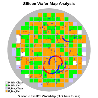
I wish the wafer map can show the shapes of the wafer edge, dies and channels between each dies, all with actual size, similar to the image attached.
Can you please provide example datasets which can be used for each functions in the toolkit?
Thank you very much.
Kind Regards
Alan
@fabengineer, I would approach this using Graph Builder and the Annotate Tool. You can create the graph with the scatter plot and then annotate the wafer map onto it. The map can show the spaces between the dies, it's called the kerf in the tool. Your litho or integration team should have the dimensions of the die including the space between the die in the reticle. They will also know how the die origin is set up which is also needed to get the layout correct.
M
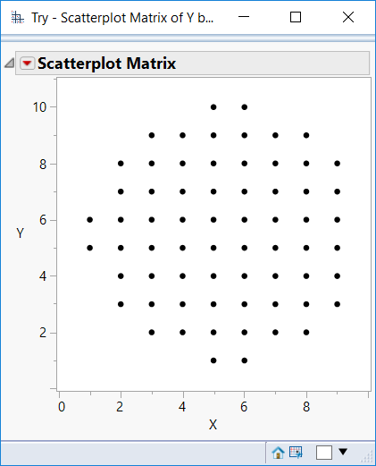
@MikeD_Anderson, I've built a scatterplot matrix as shown below. But it doesn't give any responses to the commands from the annotation tool. As you can see from the figure, the X and Y are the numbering of the die on the wafer, not in the actuall dimention, however, the parameters in the Annotate Tool are all measured with mm or um.
The SemiconductorToolkit.pdf you provided shows the introduction of each sections of the toolkit, but doesn't show the detail instructions for using each fuctions in the toll-kit. I'd like to know is there any chance you could provide a video or an instruction to demostrate the toolkit please? I've watched the tutorial as published here: https://community.jmp.com/t5/Discovery-Summit-2016/All-Wafer-Maps-Are-Wrong-An-Adventure-in-Semicond.... It shows the final results of the wafer maps but doesn't show the detail settings of the data.
I think the form of the dataset is quite important here, and the probing results are various from different probers.
If possible, can you please publish the data set which used to produce the wafer map as shown in your original post? Maybe I can adjust the form of my data to match yours to see if the mapping function works.
Thank you very much.
Create a scatter plot using the particle data. Then you would draw the die onto the map using the annotate feature.
M
Hi Mike- Lots of potential here, but I can't use any of it unfortunately until I figure out how to offset the entire die grid to match how the wafer is actually exposed. I've tried using the stepper coordinate (wafer-level coords) with an offset, however it still wants to place the (0,0) die right in the middle. Is there a way to offset the center die, and therefore the whole mapping?
Thank you.
M
I have been trying to use the Toolkit. Perhaps because we make detector chips with over 55000 die per 100mm wafer (266 rows x 272 columns), any attempts to use annotate or mapping get hung for a long time, requiring a shutdown of JMP. A typical use would be a dataset of 30-50 measurements to be turned into a low-resolution map of gross distributions for feedback to equipment engineers. We already create "standard" maps but I would like to use the extra features of the toolkit.
Hi there,
Great add-in, and I've only scratched the surface.
Couple of requests though:
1) Can the default wafer size etc be save somewhere, as I am constantly having to edit them
2) Can we have the option of a flat instead of just a notch
-all coming from someone who works in compound semi (still on small flatted wafers here :( )
M
Finally upgraded to JMP 14 to use this awesome add-in.. We currently deal with pizza masks where there are rows / columns / subrows and subcolumns. I haven't found any information how to use this with our current layout. Any suggestions?
Hello.
Today I installed JMP(V14) with Semiconductor Toolkit for wafer parametric map.
But I don't know how to start even if I refer to the attached PDF.
Is there anyone who can briefly explain step by step?
I have only 30 days to evaluate the JMP with Semiconductor Toolkit.
Thans in advance.
Best regards,
HK Jung
column
Hello
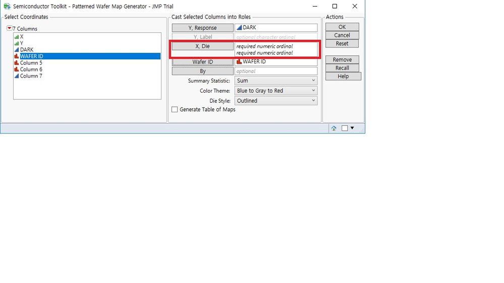
Y, Response and Wafer ID area is easily filled by my Dark and Wafer ID column.
I want to set the X, Die area with my X, Y columns data, but I can't set the X, Die area.
My X column data is X-position of die in wafer and Y column data is Y-position of die in wafer.
Please, give me any comment for this.
Thanks.
Hi, @HK_JUNG!
If it's not letting you put your die columns into the "X, Die" area it might be that they are set as character data, not numeric data. Right click on the column name (in the data table) and select column properties. The two pulldowns should be "numeric" and "ordinal."
If you're doing a 30-day trial, you should really reach out to the Systems Engineer for your region. The STK isn't official JMP software - just something I started as a passion project. So they can't provide support with the toolkit, but they can help you with the learning curve of JMP itself. This will help with learning how to use the toolkit as well. If you send me a private message with your location and email, I'll get the right people. To send me a PM, click on my username. It will open a page with a "send private message" button.
Best,
M
Hi @HK_JUNG
Thank you very much for reaching out to JMP commumity! I am Inside sales of JMP Korea and you can contact JMP Korea team directly, if you need immediate assistances. As I wrote to you by email, JMP Korea team provide Open seminars, JMP DII and free meetings and so on. For your refernces, JMP Korea Sr. Systems Engineer : ikju.shin@jmp.com. Thank you!
Recommended Articles
- © 2026 JMP Statistical Discovery LLC. All Rights Reserved.
- Terms of Use
- Privacy Statement
- Contact Us

