Level: Intermediate
John Como, Process Engineer, Intel Corp.
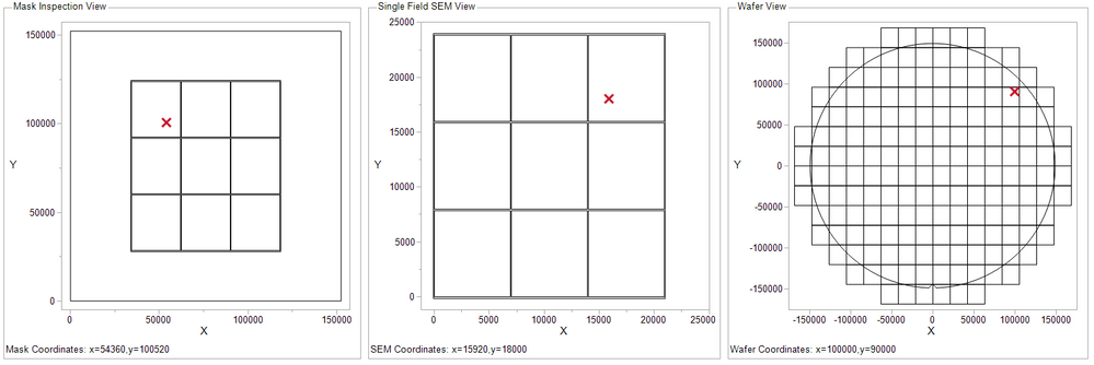
In semiconductor manufacturing, masks are used to imprint patterns onto wafers in the lithography process. The pattern dimensions on the 6" masks are 4x larger than the pattern printed on the 12" wafers, so multiple dies are printed onto a single wafer. A single defect on the mask pattern can cause a repeating bad die and cost the manufacturing company millions, so it is imperative that mask defects be found and characterized. Often times, the mask inspection machines use a different coordinate system than the wafer inspection machines, and the linear distances on the mask are 4x longer than distances on the wafers. If a defect is found on the mask, then a tedious conversion from mask to wafer coordinates must be done in order to verify if there is an effect. This interactive application written in JSL makes it simple to convert coordinates from one system to another, and even creates an image of the mask, wafer and the location of the defect for easy comparison to real-world data. This presentation will cover the mathematics behind the conversions and showcase how JSL was used to create an application to simplify the calculation.

